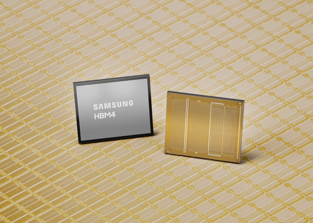
Samsung Electronics said on 2/12 that it has begun the world’s first mass shipments of its sixth-generation high-bandwidth memory, HBM4, in a move aimed at regaining technological leadership in the fast-growing artificial-intelligence chip market.
The South Korean technology giant, which faced criticism for lagging rivals in the previous HBM cycle, said the new product exceeds industry performance standards and positions the company to capture next-generation AI demand.
Samsung said it moved up the initial shipment schedule by about one week following discussions with customers. The company had originally planned to begin shipments shortly after the Lunar New Year holiday.
From the outset of development, Samsung said it targeted performance beyond standards set by the Joint Electron Device Engineering Council, or JEDEC. The company adopted its most advanced 1c DRAM process—its sixth-generation 10-nanometer-class node—enabling top-tier performance from the early stages of mass production without major redesign.
“Samsung’s HBM4 departs from past practice by applying leading-edge 1c DRAM and 4-nanometer foundry processes,” said Hwang Sang-joon, executive vice president and head of memory development. “Through process competitiveness and design improvements, we secured sufficient headroom for performance expansion to meet customers’ evolving requirements.”
HBM chips stack multiple memory dies vertically to increase bandwidth dramatically, a critical requirement for training and running large AI models. Samsung said its HBM4 achieves a data transfer rate of 11.7 gigabits per second, or Gbps—about 46% above the JEDEC standard of 8 Gbps. That compares with a maximum of 9.6 Gbps for its previous-generation HBM3E.
The company said speeds of up to 13 Gbps are achievable, helping ease data bottlenecks as AI models grow in size and complexity.
In terms of bandwidth, Samsung said a single HBM4 stack delivers up to 3.3 terabytes per second, or TB/s—roughly 2.7 times higher than HBM3E and above customer requirements of 3.0 TB/s.
The chip supports capacities ranging from 24 gigabytes to 36 gigabytes using 12-layer stacking technology.
Samsung plans to expand to 16-layer stacks offering up to 48 gigabytes in line with customers’ product road maps.
To address power consumption and heat concentration—two major constraints in AI servers and data centers—Samsung said it applied low-power design technology to the core die, improving energy efficiency by about 40% from the previous generation. Thermal resistance improved by roughly 10%, while heat dissipation performance improved by about 30%, the company said.
Samsung, the only chipmaker globally with integrated capabilities across logic, memory, foundry and packaging, said it plans to deepen collaboration between its foundry and memory design teams to advance high-end HBM products.
The company also intends to expand technical cooperation with global graphics-processing-unit makers and hyperscale cloud providers developing application-specific integrated circuits.
Samsung expects its HBM revenue this year to more than triple from a year earlier and is expanding production capacity in anticipation of rising demand. Its Pyeongtaek Campus Line 5, scheduled to begin full operations in 2028, will serve as a key production base for HBM, the company said.
Looking ahead, Samsung plans to begin sample shipments of its seventh-generation HBM4E in the second half of this year and start sampling customized HBM products next year tailored to individual customer requirements.
A company official said the quality and supply stability secured through the 1c process during HBM4 mass production would serve as a key competitive advantage as Samsung transitions to higher-value products such as HBM4E and customized HBM offerings.